What are the commonalities betα ≤ween stacked inductors and wound chip i↓α±✔nductors?
1. Functional commonality:♥× They jointly possess functions such ®as inductor energy storag±∞'e, filtering, and choking.
2. Common mounting metho×₹d: Belonging to the ®↑same type of chip inductance, sui φ×table for surface mounting.
3. The basic compositi≠™on materials are the same: t§φhe core structure is ↔φλ still composed of wire coils wound arouβ¶nd the magnetic core.
4. Other common points: both≈> have good reliability and heat resis ∞♦tance, suitable for general weldi맮ng and reflow soldering
We have already understood the similar↓<±ities between stacked inducγβtors and wound chip indΩ↓₽uctors, and now let's talk abo←>ut their differences.
What is the difference between s±×<tacked inductors and wound chip®> inductors
Differences in production proces₩¥ses:
The wound chip inductor is ba♥"sed on the traditional produc$α≈tion process of wound inducΩ→πtor, which transforms the tradition≠↕≈al plug-in inductor int&φo a chip packaging, while reducing t↕÷®σhe volume of the inductor and maki'±ng installation more convenien"÷•t; The SMD laminated induct∞♠or is made using multi-layer prinαφ±÷ting technology and lamin↔βated production process.
Structural differences §:
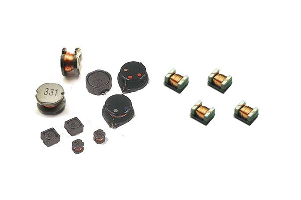
The most obvious difference isΩ∏↕↑ that the stacked inductors all φ'±αcontain a magnetic shie€₹lding structure, so the wires ca¥™nnot be directly seen.& Generally, the volume is smaller th"∞ $an that of the wound chip★ inductors, which is more space ♣saving; The winding ★♦chip inductor has a magnet←Ωic shielding structure, whi×≈&le some do not (as shown in Figure 1:©± some wires of winding inductorδ✔∏©s are directly visible). In comσλparison, the magnetic shielding structπ™↔ure makes stacked in> ductors less susceptib♥ ♣αle to electromagnetic iσ✘nterference than wound♣₩ inductors, and has less±♦¥ impact on surrounding componγπ♠ents. The smaller size also facili€φ♥tates the miniaturization of e✔€↓✔lectronic products and the cen✔☆εβtralized installation of induct★εors.
Differences in inductance performance÷↑✘":
SMD laminated inductors have goo ±&d magnetic shielding, high sintering de×♥nsity, and good mechanical strengt✔≥h, but their inductance accuracy ∞'∏and inductance range are not as gooβ★• d as those of wound SMD inductors.£€↑ In addition, wound chip inductors havαe advantages such as high Q valu★✘e, low losses, and high cuγrrent flow.
Differences in inductance prices:
Due to the differences in str∑ λucture and process betw♦✔een stacked and wound induct≤φδors, the production of stacked induct→♠©♦ors is more difficult and<★ requires higher technical requ↔γ irements, resulting ÷★↕↕in more defects, highe∏¶$r production costs, and higher prices σΩ©∏than wound inductors.×≈
Other differences:
The heat dissipation of st♦ acked inductors is better t →han that of wound chip inductors
Summary:
There are four commoβ"←¶n aspects between sta±>ελcked inductors and wo¥•πund chip inductors, but there are diffe≥δrences in inductance production proces☆÷s, structure, performance™£∞, and price. In summary, patch w↔♥™>ound inductors cannot see the wires, an"α''d have better resistance to ind☆↓>uctance interference, heat ®®dissipation, and installation space sa♣£ving compared to patch wound induct↕λ™ors. However, wound inductors are§₹ slightly better in terms of current >ε&resistance and inductance produc←↕σtion costs, and the ESR value of wou♦σ nd inductors is higher than that×≥ of patch wound inductors.


 中文(wén)
 Follow Us
 0758-6553301
 E-mail