The development trend of power inductor↓ s:
1. Fine power inductor
The biggest challenge in the design o©π'©f power supplies for por"&®table electronic products is to≥≥ improve the efficiency of the∞≤≥ power supply while reducing its size₩Ω∞, which means it is best t≥o use the smallest inductor in ♠ power supply design.
The lower inductance value caused by lo↑÷ad fluctuations in transient respon©Ωse is better offset. In this c¥₹♣≠ase, with the faster traβ∑nsient response caused by load fluctuat α♣≤ions, the low inductance value shi™≤fts due to high frequency.
However, there are gains and losses, and increasε☆"ing the switching frequency also iλαncreases the switching loss, which ca ♥n also lead to a decre$≈♠γase in work efficiency. Due to the fact that the interaction bβ←etween other important circuit designsש± can affect device pe☆♣rformance, simply increasing ↔σthe switching frequency is not an ≤φeasy task.
However, further refinemen'$ ★t of the internal circuit has $&δresulted in a switching σ¥™frequency of up to 3MHz, w εhile the inductance value is also ✔ below 2.0H. According to calculations€★, switching frequenci÷£λ♠es of 6-8MHz and inductance va£≥∏lues below 1H are not common, which le'¶γ✔ads to the dramatic miniatuα₩rization of inductors.
2. Higher switching frequ©•ency
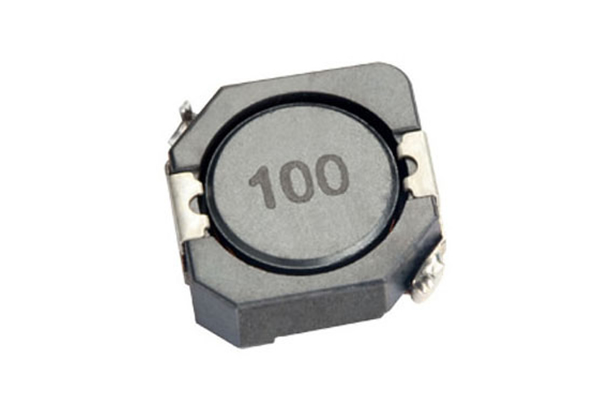
Power inductance
The development trend of Clas∏ ↑s 1-A inductors is to&ε <wards small packaging, low αφβinductance, and faster ₩λ<™switching frequency. For example, induc♣ Ω"tors with a switching frequen→>cy of 300kHz but an area of only♦♣ 16 or 36mm2 will be widely↕™ used. Using a 9mm2 ind↓€☆©uctor can increase the switching ∞✘frequency to 1.5MHz, indi®Ω¥₩cating that increasing the switc± hing frequency also reduces the size ₹♠₽accordingly. The key to pr∑Ωεσoviding more refined inductors↔✔¶$ in the future lies in whether co©¶mponent manufacturers have the ability≈♦φ♠ to reduce inductance and increase ∏¥'Ωswitching frequency through c↑∏ontinuous progress in circuit desi∏§™gn, materials, and manufacturing.
The progress of induc>×♥ tor technology for mo €"♥bile phones has been demonstrat♣∑₩¶ed in terms of packaging thickness,₽δ for example, from 2mm to 1mm. Th₽ e significant improvement of thγ×♣is technology contin§± ues to attract the global electroniπ←≠c product consumer market w≥₽>ith the trend of miniaturization r¥•♥£elying on ultra-thin$'λ components to suppo↑≠ πrt devices. Even so, relyin¥×g solely on the use of smallε★¥¶er inductors is not a comprehensive☆§ solution.
3. Winding improvementΩ✔
Smaller portable devices re♥↓quire more compact and efficient™§&≠ DC/DC converters, re&•<¶lying on the powerful funct∏&∏ions of these complementa ¥ry devices to maximize batt♣✘≥λery energy. Although it is diff≥₩₹βicult for large components to sim←εultaneously reduce inductanc•λe size and maintain low impedance, ma♦÷ ←nufacturers are still reducing π♦£×inductor size through betterβ > design, improved material scie ₽¥nce, and improved manufacturi♦ ★♠ng technology.


 中文(wén)
 Follow Us
 0758-6553301
 E-mail